RGB clock
RGB clock
This is the documentation page for the RGB clock kit.
Overview
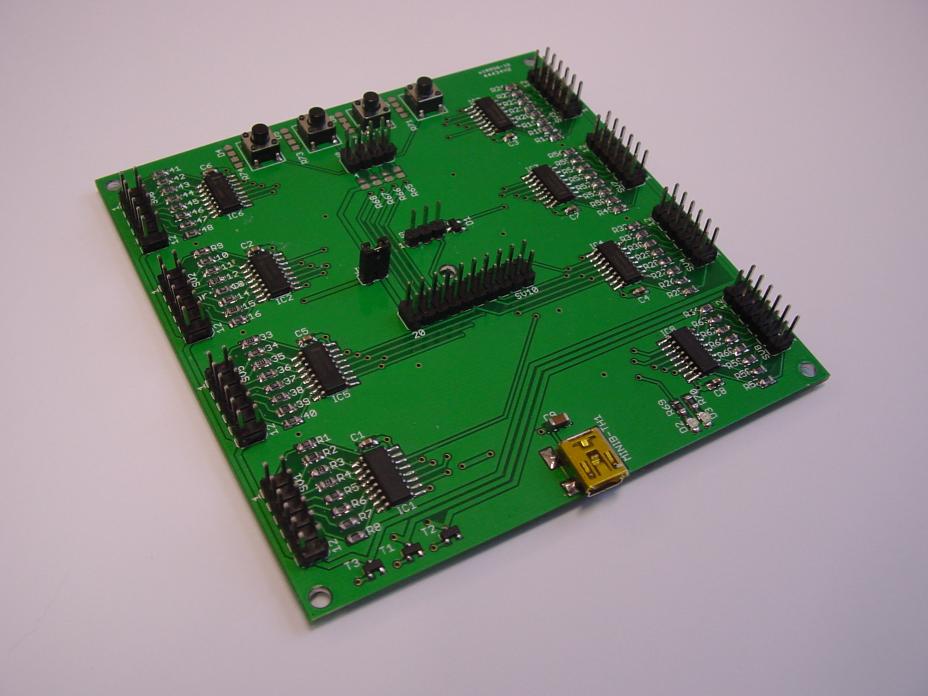
Driver PCB for up to 64 common-anode RGB LEDs, or 192 normal LEDs.
The PCB is designed for 1:3 multiplexing of the LEDs, and is equipped with 8 74HC595 shift registers (configured as 4 16-bit deep registers), 64 current-limiting resistors (220 Ohm by default) and 3 FETs to switch the cathode groups on-and-off.
The PCB is equipped with a BitWizard-standard 20-pin IO connector, designed to work together with our USB-multio PCB, but it is also possible to connect our FTDI-ATmega, USB-bigmultio or Cyclone dev board, or one of your own boards, like for example an Arduino.
SV1-SV8 are the connectors for the RGB LEDs. SV1-SV8 are connected to IC1-IC8.
IC1 and IC5 are configured as one 16-bit deep shift register. Qa-Qh are connected to IC1, and Qi-Qp are connected to IC5.
IC2 and IC6 are configured as one 16-bit deep shift register. Qa-Qh are connected to IC2, and Qi-Qp are connected to IC6.
IC3 and IC7 are configured as one 16-bit deep shift register. Qa-Qh are connected to IC3, and Qi-Qp are connected to IC7.
IC4 and IC8 are configured as one 16-bit deep shift register. Qa-Qh are connected to IC4, and Qi-Qp are connected to IC8.
The control pins (!OE, LATCH, !RESET, CLK) of all shift registers are connected in parallel.
SER0 is connected to IC1.
SER1 is connected to IC2.
SER2 is connected to IC3.
SER3 is connected to IC4.
It is therefore required to update all shift registers at the same time.
Assembling the kit
LED Driver PCB
- First, decide if you want to use 4 pushbutton switches (for the default firmware), 4 LEDs, or a mix (for custom firmware).
- SW1 and R65 or D7 and R71
- SW2 and R66 or D6 and R72
- SW3 and R67 or D5 and R73
- SW4 and R68 or D4 and R74
- Mount all necessary SMD components. Which component should go where, can be found in the table below.
- cut the header strips to the right length. Our suggestion:
- cut the first strip in one 10-pin long strip, and 5 6-pin long strips.
- cut the second header in 3 6-pin strips, and one 4-pin strip.
- solder all headers in place
- solder the desired switches in place
Component   Value
IC1-IC8     74HC595
R1-R64      220R
R65-R68     10K
R69-R74     1K
C1-C8       100nF
C9          10uF
T1-T3       N-channel FET
D1          Double Diode (BAT54S for example)
D2-D7       LED
SW1-SW4     Pushbutton
LED chains
Building your own clock-face
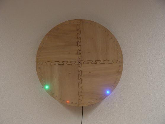
If you are not buying the laser-cut clock-face that we offer, you'll be building one yourself. A consideration is that at about 20cm radius, the legs of the leds are long enough to form the R, G and B common lines. If you make the clock larger, you'll have to run three wires along the leds....
The "puzzle" line between the four segments stems from the fact that the laser-cutter that we have access to only goes so big. And it comes in handy for transport. The laser-cutter could handle up to 30cm outer diameter. And it could handle half a clock at once. But the 4-fold symmetry looks nice.
Connecting the LEDs
Counting clockwise, starting at the LED to the right of the topmost LED:
Output  Pin#  Connector
Qp      8     SV6
Qo      7     SV6
Qn      6     SV6
Qm      5     SV6
Ql      4     SV6
Qk      3     SV6
Qj      2     SV6
Qi      1     SV6
Qg      7     SV2
Qf      6     SV2
Qe      5     SV2
Qd      4     SV2
Qc      3     SV2
Qb      2     SV2
Qa      1     SV2
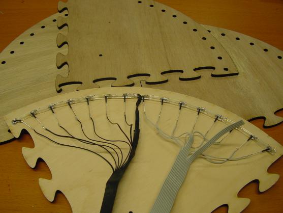
All R, G and B pins should be connected in parallel.
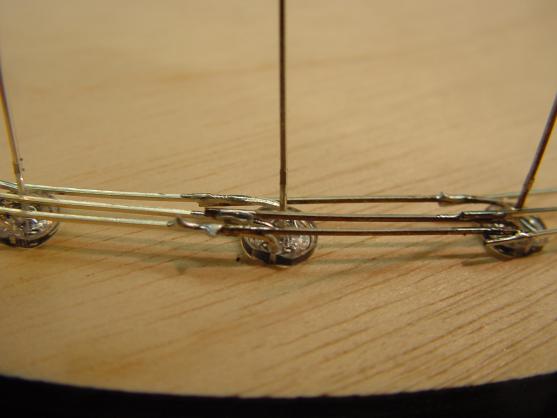
This is the same for each quadrant, only the connector numbers differ.
Putting it all together
Version 1.0 uses 12pin headers to connect to the LEDs, but unfortunately, 12-pin ICD connectors don't exist, so we used 14-pin ICD connectors.
Pay close attention then connecting the 14-pin connectors to the PCB! Pin 1 through 12 should line up, and pin 13 and 14 should be "floating".
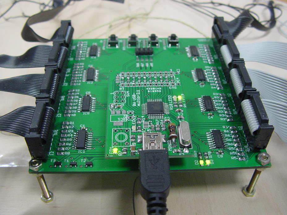
As can be seen in this image, the left ICD connectors are a bit further towards the USB connector, and the right ICD connectors are a bit further to the switches.
After hooking everything up, you should end up with something like this:
External resources
Pinout
SV10 is connected as follows
| connector pin number | pin name | multiio AVR pin name |
|---|---|---|
| 1 | GND | |
| 2 | GND | |
| 3 | SER0 | PD1 |
| 4 | SER1 | PD2 |
| 5 | SER2 | PD3 |
| 6 | SER3 | PD4 |
| 7 | !OE | PD5 |
| 8 | LATCH | PD6 |
| 9 | !RESET | PB1 |
| 10 | CLOCK | PB0 |
| 11 | R | PB3 |
| 12 | G | PB2 |
| 13 | B | PB5 |
| 14 | external clock source | PB4 |
| 15 | IO1 | PB7 |
| 16 | IO0 | PB6 |
| 17 | IO3 | PC6 |
| 18 | IO2 | PC7 |
| 19 | VCC | |
| 20 | VCC |
SV1 through SV8 are connected as follows:
| 1 | A0 |
| 2 | A1 |
| 3 | A2 |
| 4 | A3 |
| 5 | A4 |
| 6 | A5 |
| 7 | A6 |
| 8 | A7 |
| 9 | R |
| 10 | G |
| 11 | B |
| 12 | GND |
SV9 can be used to connect an external clock source, or a servo motor, or...
| 1 | GND |
| 2 | VCC |
| 3 | connected to pin14 of SV10 |
Pin 3 has two clamping diodes attached, to limit the voltage range to GND-0.6V and VCC+0.6V.
We are considering connecting this pin through a very large valued resistor directly to the mains. In that case the clamping diodes are neccessary. The better option would be to use an optocoupler or something like that....
Leds:
- D2 is connected to VCC from SV10
- D3 is connected to USB power
- D4 is connected to pin17 from SV10
- D5 is connected to pin18 from SV10
- D6 is connected to pin15 from SV10
- D7 is connected to pin16 from SV10
Switches:
- Switch1 (next to R71) is connected to pin16 from SV10
- Switch2 (next to R72) is connected to pin15 from SV10
- Switch3 (next to R73) is connected to pin18 from SV10
- Switch4 (next to R74) is connected to pin17 from SV10
Jumper settings
JP1: Power supply selection.
Open: LED driver board and microcontroller board have individual power supplies
Closed: VCC from LED driver board and microcontroller board are connected.
alternative use
- If the complete device is powered from the microcontroller board, the jumper can be replaced with a toggle switch. This allows you to turn the LEDs on and off, without affecting timekeeping. (Untested: Possibly the charging of the capacitor on the PCB will cause a brownout on the MCU board. :-( . Solutions are: decrease the value of the capacitor on the RGB clock board, increase the value of the capacitor on the multiio board, or patch the capacitor on the RGB board to be connected to the "from the controller board" signal instead of to the "local power" signal.)
- If you want to measure the powerconsumption of the leds, you can connect your ammeter here.
The software
The software supplied by BitWizard, is designed to run on the BitWizard Multio board, but it should be possible to port it to other boards. A link to the sources will be posted within a few days (It's Jan 9th 2012 at the moment).
Default operation
Setting the time
The current firmware enables you to set the time over a USB-serial port, using the "T" command.
Usage:
T [hh] [mm] [ss]
With hh, mm, and ss in hexadecimal. For example:
T 10 2F D
sets the time to 16:47:13 .
At BitWizard, we use the following script (we called it tsync) to set the time:
#!/bin/sh
h=`(echo obase=16 ;date +"%H" )| bc`
m=`(echo obase=16 ;date +"%M" )| bc`
s=`(echo obase=16 ;date +"%S" )| bc`
echo T $h $m $s
Forward the output of this script to the clock, to set the time:
./tsync > /dev/ttyACM0
Reading back the time
The "t" command outputs the current time on the clock over the serial interface:
CDC usbio/usbmultiio Wed Jan 11 18:28:22 CET 2012
> t 11:2F:03.02E0
>
The time is printed in hex, in hh:mm:ss:milliseconds
Adjusting the white-balance
Setting the white-balance can be done with the "B" command.
Usage:
B [rValue] [gValue] [bValue]
Values are in hex. Example (this is the default setting):
B 7800 7E00 0000
This means the red LED is on from 0x0000 until 0x7800, green is on from 0x7800 until 0x7E00, and green is on from 0x7E00 until 0x0000.
This counter counts from 0x0000 to 0xBB80.
Jump to bootloader
If you want to flash the controller, you need to switch to the bootloader. You can do this by pressing the pushbutton, of if you're lazy (or if the clock is hanging on a wall on the other side of the room) you can do it by issuing the "z" command.
Future hardware enhancements
- Replace 2 12-pin connectors by 1 20-pin connector
- Add numbers to the pushbutton switches
Changelog
1.0
- Initial public release
